The Nobel Prize in Physics in the year 2000 went to engineers Jack Kilby and Robert Norton Noyce for their participation in the invention of the integrated circuit. Trying to tackle the problems brought about by the increasing complexity of computers, both had come at the same time, in the late 1950s, to an equivalent solution using two different materials, allowing a miniaturization and compaction of discrete electronics that revolutionized the world of electronics. Kilby used germanium, while Noyce used silicon. This second material was the winner of the battle due to its abundance and, for the last fifty years, has been the basis of integrated circuits has been made out of silicon. This element is the second most abundant in the Earth, and we can find it in window glass and in the sand on our beaches.
Despite using the same principle since their invention, transistors, one of the most common components of integrated circuits, have changed a lot, especially in size. The first transistors measured 0.01 millimetres, while now they barely reach 10 nm, almost 10,000 times smaller.
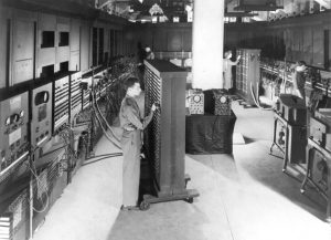
This has led to an increase in the processing power of electronic devices while reducing their size. To get an idea, the ENIAC, considered as the first computer, occupied an entire room and weighed 27 tons. Its computing power was around 5,000 sums per second, a thousand times slower than the processing power of the phones we use nowadays. However, despite the success of this technology, we are reaching its limit. Someday it will be physically impossible to reduce the size of transistors any further, because we cannot make them smaller than an atom. At the same time, reducing the size of integrated circuits causes other types of problems with the copper cables through which the electric current circulates.
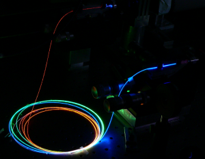
Among the limitations of copper cables are: the limit on bandwidth, that is, the amount of information that we can transmit over these cables per unit of time; current losses and interference between nearby cables; the heat dissipation of these cables, and also the space they occupy. One of the possible solution to all these problems could be found in integrated photonics, which, instead of using electrons and copper cables, uses photons (that is, light) and optic fibers to transmit the information, with the great advantage of having a greater bandwidth and faster speed in the transmission of information: the speed of light!
In industrial processes, the cost of production is also very important. What would be the cost of replacing the already existing technology? This situation is one of the biggest obstacles to the implementation of integrated photonics. However, the use of silicon-based photonics can be the solution. This technology can be produced with the same industrial processes already in use for electronic microchips manufactured today. It only needs small modifications of their designs to transmit light instead of electrons. In fact, this is something we are already doing, using them, among other applications, for interconnected data, supercomputers, and sensors, either to diagnose diseases or detect explosives.
However, this technology also has its drawbacks. Silicon is a good light transmitter but a very poor light emitter. So, we have something that behaves very well as a copper wire in our simile with electrons, being transparent to infrared light in the so-called “telecommunications band”, but today we do not have a silicon-based light emitter. The silicon has what is know as an indirect band gap. The band gap is called direct if an electron can directly emit a photon. In an indirect gap, a photon cannot be emitted because the electron must pass through an intermediate state and transfer momentum to the crystal lattice losing energy and heating up in the process.
In one of the projects I am participating in as a researcher with researchers from McMaster University in Canada, the University of Salford and the University of Manchester in the United Kingdom, we seek to modify germanium, precisely the compound with which some of the first transistors were made, so that it emits light in the same frequency band in which silicon is transparent and can transmit it.
Germanium is not a good light emitter in this band either as it has an indirect band gap. However, its indirect transition is smaller than the one for silicon and, therefore, it is easier to modify it so that it becomes direct transition, thus achieving light emission. These modifications in the properties of the materials can be carried out in many different ways, from adding ions of different elements, to changing their temperature or, as in our case, creating tensions in the material that deform its crystalline structure which modifies its optical properties.
Much remains to be studied in this field, both in technical engineering and in its stability. However, both our studies and those of other groups are beginning to give promising results that lead us to think that the future of communications could come in the hand of integrated photonics.
* * *
By Laura Martínez Maestro (@Laurawendy), Lecturer in Physics at the School of Computing, Science and Engineering at the University of Salford.
More information:


.jpg)